锐峰先科技术有限公司
BE FIRST TECHNOLOGY CO., LTD
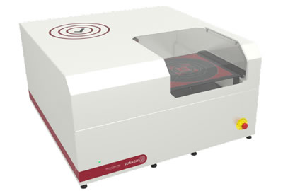
SURAGUS EddyCus TF map 2530
|
EddyCus TF map 2530 Series – Non-contact Sheet Resistance and Metal Layer Thickness Mapping Device
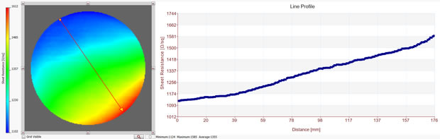
The EddyCus TF map 2530 Series automatically measures the sheet resistance of large samples up to 300 x 300 mm² (12 x 12 inches) in non-contact mode. Upon manual sample positioning the device automatically measures and displays an accurate mapping of the sheet resistance across the entire sample area. The measurement settings allow easily and flexibly to choose between fast measurement times of below 1 minute or high spatial measurement resolution of more than 100,000 measurement points.
Highlights · Non-contact
Characteristics · Technology: non-contact eddy current
Applications Coated architectural glass, e.g. LowE |