Service Hotline:400-9988-118

锐峰先科技术有限公司

BE FIRST TECHNOLOGY CO., LTD

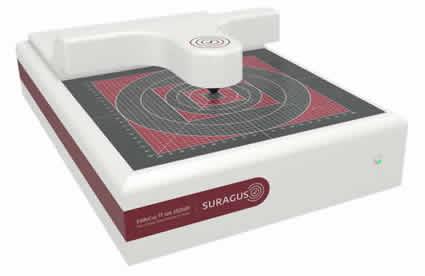
SURAGUS EddyCus TF lab 2020


Non-contact sheet resistance and layer thickness measurement device for single point measurements


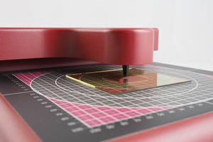
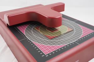
The EddyCus TF lab 2020 allows manual single point measurements of conductive thin films and layer thickness measurement of thin metal layers in non-contact mode. The compact bench-top device is ideal for fast and accurate measurements of samples up to 200 x 200 mm2 (8 x 8 inches). In addition to the measurement of thin conductive layers also doped wafers and conductive polymers can be analyzed.


Advantages:

• Non-contact real time measurement
• Precise measurement of conductive thin films
• Characterization of hidden and encapsulated conductive layers
• Measurement data saving and export functions


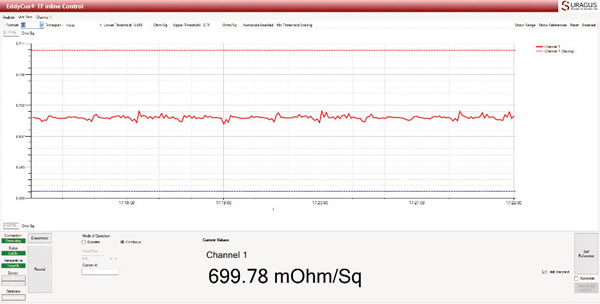
Measurement characteristics:

Sheet resistance
Thickness measurement of metal layers
Single point measurement
Quality control, input and output control
Sample sizes: 10 x 10 mm2 to 200 x 200 mm2 (0.5 x 0.5 inches to 8 x 8 inches)
Measurement range: 0.001 to 3,000 Ohm/sq


Applications:

• Coated architectural glass, e.g. LowE
• Displays, touch screens and flat panel displays
• OLED and LED applications
• Smart glass
• Graphene layers
• Photovoltaic wafers and cells
• Semiconductor wafers
• Metallization layers and wafer metallization
• De-icing and heating applications
• Battery electrodes
• Conductively coated paper and conductive textiles


Software and device control

Very user-friendly software
Intuitive, touch display navigation
Real-time measurement of sheet resistance and layer thickness
Software-assisted manual mapping option
Various data saving and export options