锐峰先科技术有限公司
BE FIRST TECHNOLOGY CO., LTD
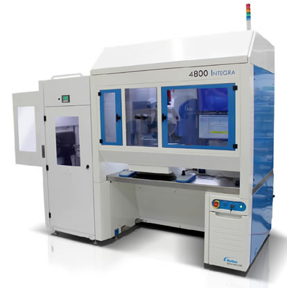
DAGE 4800 INTEGRA Plus Automated Bondtester
|
Next Generation automated bond tester for wafer-level packaging
The 4800 INTEGRA Plus is the next generation automated bond test solution designed to meet the dynamic wafer-level packing environment. With its new motion, vision, and wafer handling system complemented by the high-throughput Paragon software, the system offers best-in-class micro bump and trace bond testing on chip-on-wafer, stacked wafer, and molded wafer applications. The system demonstrates unmatched precision, hands-free, and fully traceable bond testing capability for both 200 and 300mm wafers enabled by a smart load port and wafer chuck, and Matrix Map software. Ready for the next step of automation using Nordson Intelligence for easy Autograding routines.
The Nordson TEST & INSPECTION's Bondtest 4800 INTEGRA is a complete solution for automated semiconductor wafer bond testing. INTEGRA is designed for maximum throughput in an operator free environment. It is our most advanced quality control tool.
Wafer Handler Integration
Integration with a wafer handler transforms the 4800 INTEGRA into a fully automated system ensuring reliable and repeatable operation, utilizing the latest generation of bond testing software, Paragon™. The highly intuitive and configurable interface provides quick and easy automated test routine development and execution for a wide range of sample configurations. A step by step wizard guides the user through the set up process, catering for a variety of options. Paragon™ also provides the ability to simultaneously display and record the view from multiple cameras
Successfully Test Warped and Thin Wafers
The edge lift smart chuck has a unique design where the edge lift pins ensure that warped or thin wafers cannot slide off the chuck. The gradual vacuum pressure enables optimum vacuum on the wafer. |